
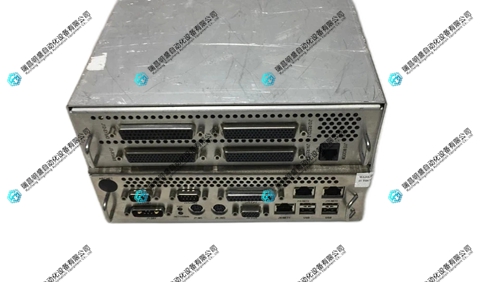
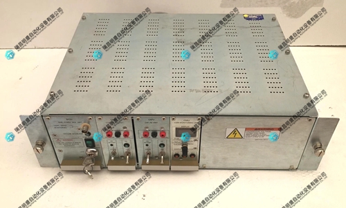
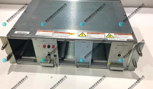


KLA Tencor 720-21216-003扫描仪模块
1.产 品 资 料 介 绍:
中文资料:
KLA Tencor 720-21216-003 扫描仪模块(Scanner Module) 是专为KLA Tencor高端半导体晶圆检测与量测设备设计的关键组成部分,负责在高精度平台上实现光学或激光扫描运动。它通常应用于**晶圆表面检测系统(如Surfscan、e-beam 或 AOI 系统)**中,是系统实现亚微米级定位与图像采集的核心组件之一。
一、产品基本信息
产品型号:720-21216-003
产品类型:扫描仪模块(Scanner Module)
制造商:KLA Tencor
所属平台:720系列晶圆检测与量测设备
功能定位:实现高速、高精度的扫描运动,配合图像采集与缺陷识别系统工作
二、核心功能与作用
| 功能类别 | 说明 |
|---|---|
| 扫描控制 | 实现平台或光学组件的线性或螺旋式扫描,确保图像覆盖整片晶圆表面。 |
| 位置反馈 | 内置编码器/激光干涉仪反馈系统,实现闭环控制,提升定位精度。 |
| 同步触发 | 配合相机或激光传感器,精确触发图像采集或数据记录。 |
| 动态调整 | 能根据系统指令动态调整扫描速度、加速度、路径和步进间隔。 |
三、应用领域
1. 晶圆缺陷检测系统(Wafer Inspection)
控制检测头或载片平台的扫描路径,确保整片晶圆被覆盖检测。
与光源、成像头、数据处理系统紧密配合,支持高速移动与高频采样。
2. 光学量测系统(Metrology Tools)
用于精准测量晶圆厚度、粗糙度、形貌等几何特性。
在Z轴或倾斜轴方向提供高分辨率控制能力。
3. e-beam 或激光成像设备
控制束斑(beam spot)在晶圆上的扫描,适用于高对比度图像采集与电性能评估。
4. 自动光学检测(AOI)平台
实现快速扫描成像,识别颗粒污染、刮痕、刻蚀缺陷等微米/亚微米级缺陷。
英文资料:
The KLA Tencor 720-21216-003 Scanner Module is a key component designed specifically for KLA Tencor's high-end semiconductor wafer inspection and measurement equipment, responsible for achieving optical or laser scanning motion on high-precision platforms. It is commonly used in wafer surface inspection systems such as Surfscan, e-beam, or AOI systems, and is one of the core components for achieving sub micron level positioning and image acquisition in the system.
1、 Basic Product Information
Product model: 720-21216-003
Product type: Scanner Module
Manufacturer: KLA Tencor
Platform: 720 Series Wafer Inspection and Measurement Equipment
Functional positioning: Achieve high-speed and high-precision scanning motion, working in conjunction with image acquisition and defect recognition systems
2、 Core functions and roles
Function category description
Scanning control enables linear or spiral scanning of the platform or optical components to ensure that the image covers the entire wafer surface.
Position feedback with built-in encoder/laser interferometer feedback system, achieving closed-loop control and improving positioning accuracy.
Synchronize triggering with cameras or laser sensors to accurately trigger image acquisition or data recording.
Dynamic adjustment can dynamically adjust scanning speed, acceleration, path, and step interval according to system instructions.
3、 Application Fields
1. Wafer Inspection System
Control the scanning path of the detection head or wafer platform to ensure that the entire wafer is covered for detection.
Closely integrated with the light source, imaging head, and data processing system, supporting high-speed movement and high-frequency sampling.
2. Optical measurement system (Metrology Tools)
Used for precise measurement of geometric characteristics such as wafer thickness, roughness, and morphology.
Provide high-resolution control capability in the Z-axis or tilt axis direction.
3. E-beam or laser imaging equipment
Control the scanning of beam spot on the wafer, suitable for high contrast image acquisition and electrical performance evaluation.
4. Automatic Optical Inspection (AOI) Platform
Realize fast scanning imaging to identify micro/sub micron level defects such as particle contamination, scratches, and etching defects.
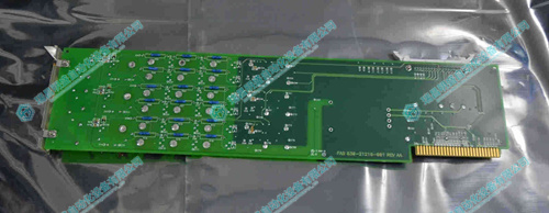
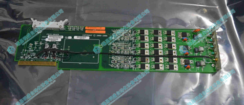
2.产 品 展 示
3.其他产品
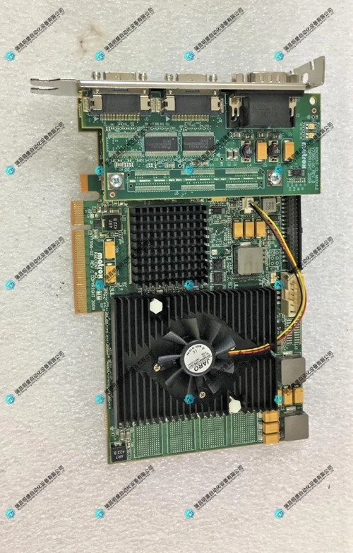
4.其他英文产品
Radisys EPC-3307 processor board
| T21NRLD-LNN-NS-00 | 6SC6170-0FC01 | 6ES5451-4UA12 |
| T21NRLC-LNN-NS-00 | GESPAC GESDMC-2 | 6ES5135-3UA11 |
| T21NRHJ-LNN-NS-00 | 6SC6100-0GA12 | 3500/32M 149986-02 |
| T21NLLC-LNN-NS-00 | CACR-SR15BB1CS | 6ES5441-8MA11 |
| T Series | CACR-SR30SF1BSB-Y124 | UIMC |
| STF5372-3750-61-82BC | SC402048001 | 61-0159-00 |
| STF5356-3749-61-45BC | SC403-014-T5 | SC933NN-050-01 |
The content is from Ruichang Mingsheng Automation Equipment Co., LTD
Contact: +86 15270269218