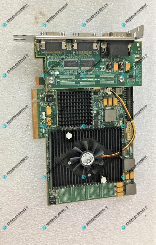
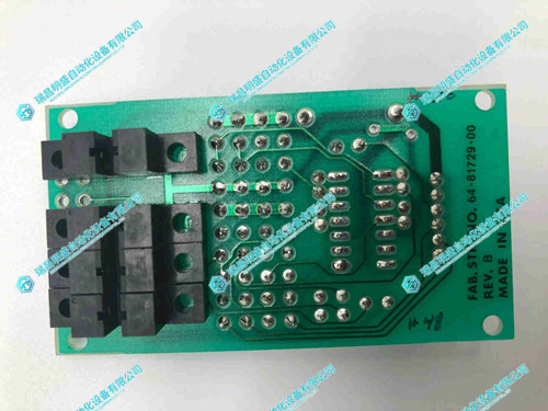


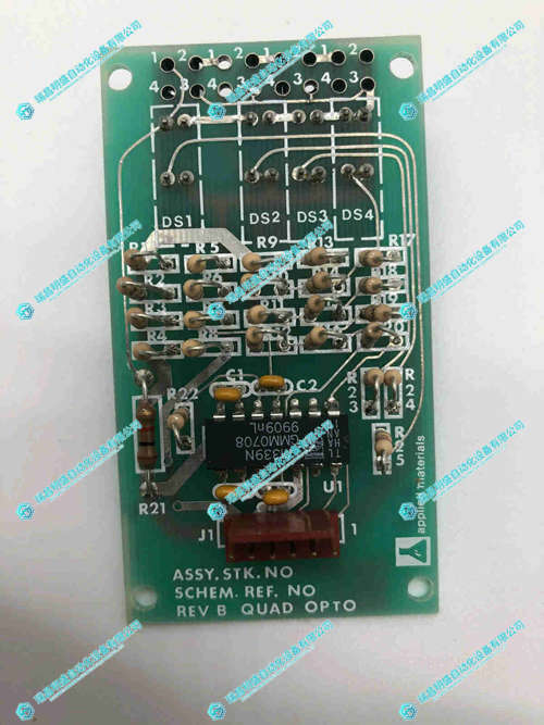
AMAT Applied Materials 03-81729-00激光探测器
1.产 品 资 料 介 绍:
- 高精度光谱响应:聚焦半导体制造常用激光波段(如红外或深紫外区域),参考同类 MCT 红外探测器的性能指标,其光谱响应范围可能覆盖 4-12μm,峰值探测率(D*)或达 10⁹-10¹¹ cm・Hz¹/²/W 级别,可实现微弱激光信号的精准捕捉。
- 快速响应与低噪声:针对半导体制造的高速生产需求,响应时间或低于 3ns,搭配低噪声放大电路设计,能实时反馈激光能量波动,适配晶圆缺陷检测等高频次监测场景。
- 工业级环境适配:采用铝 + PC 等耐用材质,工作温度范围可能覆盖 - 20~60℃,湿度耐受≤65% RH,防护等级达 IP65 以上,可适应半导体洁净车间的严苛环境。
- 系统集成兼容性:作为 AMAT 设备的原装部件,其接口设计(如 SMA 射频输出)与控制逻辑需与沉积、刻蚀等主设备无缝衔接,支持设备整体的自动化调控。
- 晶圆制造过程监测:在化学气相沉积(CVD)、物理气相沉积(PVD)等工艺中,实时监测激光干涉信号,分析薄膜厚度与均匀性,确保材料沉积精度。
- 缺陷检测与计量:配合晶圆检查设备,通过激光反射 / 散射信号分析,识别微米级表面缺陷,支撑芯片良率提升,适配人工智能、5G 芯片等高端制造需求。
- 激光光源校准:作为标准探测单元,用于设备内置激光源的能量校准与稳定性监控,保障刻蚀深度、离子注入剂量等关键工艺参数的准确性。
AMAT Applied Materials 03-81729-00激光探测器 英文资料:
1、 Core positioning and system of the product
03-81729-00 Laser detector is a key component in the semiconductor manufacturing equipment ecosystem of Applied Materials Company (AMAT), belonging to its core "Inspection and Measurement System" product line. As a precise monitoring unit in the entire process of semiconductor wafer manufacturing, this detector mainly serves the laser signal capture and analysis in chip production, supporting the quality control of multi ring joints from material deposition to etching, and is an important component to ensure chip yield.
2、 Speculation on core functions and technical characteristics
Based on the technical direction of AMAT and the industry standard for laser detectors, this product is likely to have the following characteristics:
High precision spectral response: Focusing on the commonly used laser bands in semiconductor manufacturing (such as infrared or deep ultraviolet regions), referring to the performance indicators of similar MCT infrared detectors, its spectral response range may cover 4-12 μ m, with peak detection rate (D *) or up to 10 ⁹ -10 ¹¹ cm · Hz ¹/²/W level, which can achieve precise capture of weak laser signals.
Fast response and low noise: Targeting the high-speed production needs of semiconductor manufacturing, the response time may be less than 3ns, coupled with low-noise amplifier circuit design, it can provide real-time feedback on laser energy fluctuations and adapt to high-frequency monitoring scenarios such as wafer defect detection.
Industrial grade environment adaptation: Made of durable materials such as aluminum and PC, the working temperature range may cover -20~60 ℃, the humidity tolerance is ≤ 65% RH, and the protection level is above IP65, which can adapt to the harsh environment of semiconductor cleanrooms.
System integration compatibility: As an original component of AMAT equipment, its interface design (such as SMA RF output) and control logic need to be seamlessly integrated with the main equipment such as deposition and etching, supporting the overall automation control of the equipment.
3、 Typical application scenarios
Based on the core business layout of AMAT, the application of this detector is focused on three major areas:
Wafer manufacturing process monitoring: Real time monitoring of laser interference signals in processes such as chemical vapor deposition (CVD) and physical vapor deposition (PVD), analyzing film thickness and uniformity to ensure material deposition accuracy.
Defect detection and measurement: In conjunction with wafer inspection equipment, micro level surface defects are identified through laser reflection/scattering signal analysis, supporting chip yield improvement and adapting to high-end manufacturing needs such as artificial intelligence and 5G chips.
Laser source calibration: As a standard detection unit, it is used for energy calibration and stability monitoring of the built-in laser source in equipment, ensuring the accuracy of key process parameters such as etching depth and ion implantation dose.
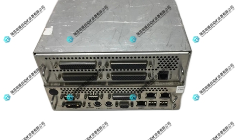
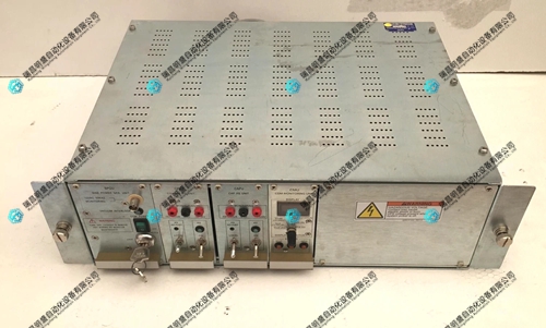
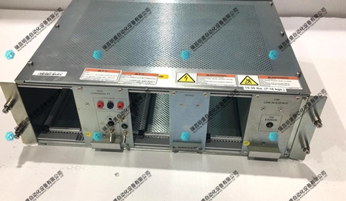
AMAT Applied Materials 03-81729-00激光探测器 产品展示
产品视频
3.其他产品
ABB TU846 终端单元
ABB SPHSS13 伺服模块
ABB SM810K01 3BSE030928R1总线互连模块
4.其他英文产品
DSMC112 57360001-HC DCS system module
DSPC174 3BSE005461R1 Logic control card
DSRF180A 57310255-AV Control framework
| 6ES5704-4CB00 | CACR-SR10SF1BFB | ATCA-4745 |
| 6ES5704-3BC50 | CACR-SR06TZ9SM-Y01A | EPC8-DX66-00-2 |
| 6ES5703-5CC00 | CACR-IR10SE | 115970-010,440 |
| 6ES5703-3CD20 | CACR-IR | 859-8150-002 |
| 6ES5703-1CC01 | CACR-SR44BC!CSY414A | PRE-913423 |
| 6ES5703-1BF00 | CACR-IR010101F | VM7830SYS |
The content is from Ruichang Mingsheng Automation Equipment Co., LTD
Contact: +86 15270269218