
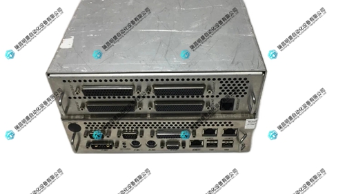
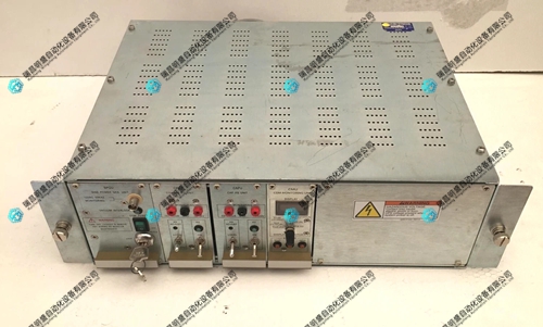
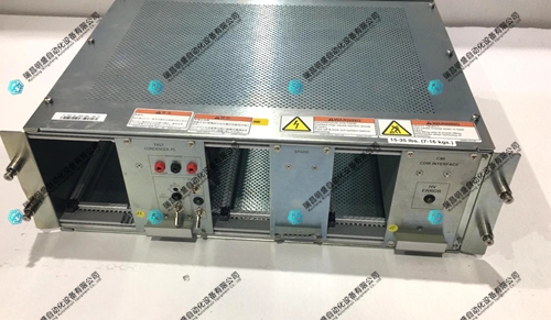
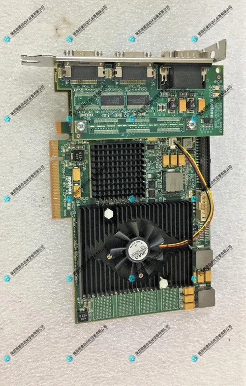
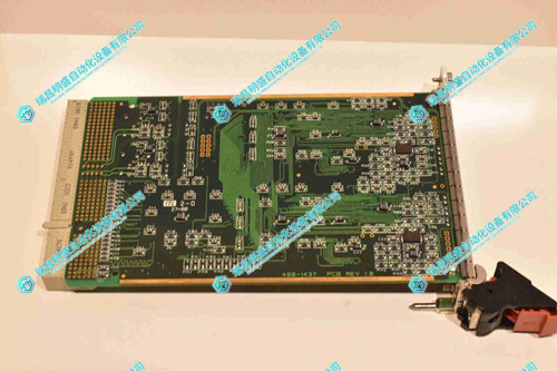
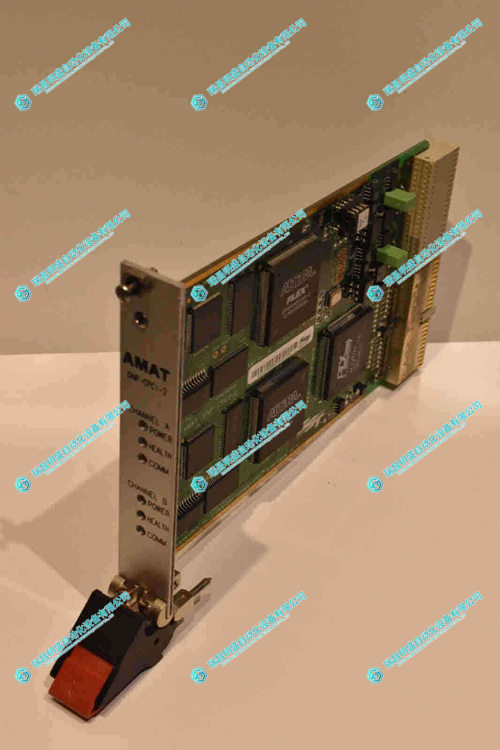


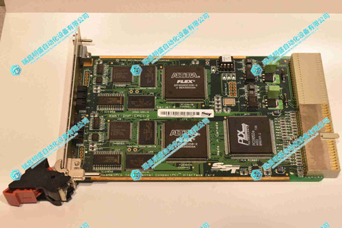
AMAT Applied Materials DNP-CPCI-2扫描仪模块
1.产 品 资 料 介 绍:
- 晶圆图案验证:适配光刻后晶圆的线宽(CD)测量与图案对准检测,通过扫描成像验证光刻工艺精度
- 缺陷检测与分类:用于刻蚀、沉积制程后的晶圆表面检测,识别划痕、颗粒、膜层缺陷等异常特征
- 掩模质量检测:对光刻掩模表面的微观缺陷进行扫描成像,保障掩模图案完整性与精度
AMAT Applied Materials DNP-CPCI-2扫描仪模块 英文资料:
1、 Product core positioning
AMAT DNP-CPCI-2 is a high-precision scanner module with CPCI bus architecture specially designed by Applied Materials for high-end semiconductor process inspection. It is the core imaging component of the wafer defect detection and pattern verification system. Its core function is to convert the microscopic patterns and defect features on the wafer surface into digital image data through high-precision optical scanning and electronic signal conversion. Combined with algorithms, it realizes size measurement, defect recognition, and process consistency verification, and is a key detection equipment to ensure semiconductor manufacturing yield.
Unlike general document scanners, this module adopts a semiconductor grade optical system and CPCI industrial bus design, with sub micron imaging accuracy and high-speed data transmission capability. It can adapt to harsh environments in clean workshops and meet the detection needs of advanced processes up to 14nm.
2、 Key technical parameters (derived from industry standards and similar products)
Based on the technical specifications of AMAT testing equipment, CPCI bus standards, and general requirements for semiconductor scanning equipment, the core specifications of this model are speculated as follows:
Parameter category
Specification Description
Optical scanning core
Adopting a high-sensitivity CCD sensor with an optical resolution of ≥ 2000dpi; Equipped with LED cold light source, spectral range of 400-700nm, no thermal radiation effect
Scanning performance characteristics
Scanning speed ≥ 50mm/s (at 1000dpi resolution); Defect detection accuracy ≤ 0.1 μ m, supporting black and white, grayscale (16 bit), and color imaging modes
Bus and Data Transmission
Adopting CPCI 2.2 standard bus interface, data transmission rate ≥ 133MB/s; Support DMA direct data transfer to reduce CPU load
Physical and Environmental Specifications
Dimensions comply with 3U CPCI standard (160 × 100 × 32mm), weight<500g; operating temperature 0-50 ℃, humidity<85%, no condensation, cleanliness Class 10 requirements
Protection and Certification
Surface anti-static coating, interface with dust-proof sealing design; Compliant with UL 61010-1 safety standards and CE electromagnetic compatibility certification
3、 Application scenarios and adaptation systems
1. Core application areas
As the "visual core" of semiconductor inspection, this scanner module mainly serves the critical inspection process:
Wafer pattern verification: adapted to measure the line width (CD) of the wafer after photolithography and detect pattern alignment, verifying the accuracy of the photolithography process through scanning imaging
Defect detection and classification: used for surface inspection of wafers after etching and deposition processes, identifying abnormal features such as scratches, particles, and film defects
Mask quality inspection: Scanning and imaging of micro defects on the surface of photolithography masks to ensure the integrity and accuracy of mask patterns
AMAT Applied Materials DNP-CPCI-2扫描仪模块 产品展示
产品视频
3.其他产品
METSO D201189L 模拟输入模块
FOXBORO FBM218/237 P0916QD 冗余适配器
Triconex 3624 数字输出模块
4.其他英文产品
BENTLY 3500/32 125712-01 Relay module
BENTLY 3500/40M 140734-01 Machinery Monitoring System
BENTLY 3500/92 136180-01 Communication gateway module
| 710-650094-20 | 8030-CRM-230 | 740-607108-005 |
| 710-650044-20 | 8030-CRM-222 | 710-611867-000 |
| 710-615775-000 | 8030-CRM-220 | F31X170TBSACG1 |
| 710-613084 | 8030-CRM-214 | 073-655007-00 |
| 710-611725-002 | 8030-CRM-211R | 531X309SPCAHG1 |
| 710-610801-001 | 531X111PSHAPG3 | F31X111PSHARG1 |
| 710-610522-000 | 193X741ACG01 | 710-661726-00 |
| 710-609995-003 | 193X801DAG01 | 710-611487-001 |
The content is from Ruichang Mingsheng Automation Equipment Co., LTD
Contact: +86 15270269218